Overview
Nanotechnology is science, engineering, and technology conducted at the nanoscale, which is about 1 to 100 nanometers. One nanometer (nm) is one-billionth or (10-9) of a meter. Nano-science and nanotechnology are the study and application of tiny things. They can be used across all the other science fields, such as chemistry, biology, physics, materials science, and engineering. Areas of physics such as nanoelectronics, nanomechanics, nanophotonics, and nanoionics have evolved during the last few decades to provide a basic scientific foundation for nanotechnology.
Approaches are used in nanotechnology
1. Top-down approach: In this approach, nano-objects are constructed from larger entities without atomic-level control.
2. Bottom-up approach: In this approach materials and devices are built from molecular components that assemble themselves chemically by principles of molecular recognition.
The ideas and concepts behind nanoscience and nanotechnology started with a talk entitled “There’s Plenty of Room at the Bottom” by physicist Richard Feynman at an American Physical Society meeting at the California Institute of Technology (CalTech) on December 29, 1959. Feynman described a process in which scientists would be able to manipulate and control individual atoms and molecules.
Note: Size distribution, specific surface feature, and quantum size effects are the principal factors that cause the properties of nanomaterials to differ significantly from other materials.
Nanomaterials unique properties
- Interface and colloid science have given rise to many materials that may be useful in nanotechnologies, such as carbon nanotubes and other fullerenes, and various nanoparticles and nanorods.
- Nanomaterials with fast ion transport are related also to nanoionics and nanoelectronics.
- Progress has been made in using these materials for medical applications such as Nanomedicine.
- Nanoscale materials such as nanopillars are sometimes used in solar cells that combat the cost of traditional silicon solar cells.
- Development of applications incorporating semiconductor nanoparticles to be used in the next generation of products, such as display technology, lighting, solar cells, and biological imaging.
- The recent application of nanomaterials includes a range of biomedical applications, such as tissue engineering, drug delivery, and biosensors.
Atomic force microscopy (AFM)
Atomic force microscopy (AFM) or scanning force microscopy (SFM) is a very high-resolution type of scanning probe microscopy (SPM), with demonstrated resolution on the order of fractions of a nanometer, more than 1000 times better than the optical diffraction limit.
The AFM has three major abilities:
- In force measurement, AFMs can be used to measure the forces between the probe and the sample as a function of their mutual separation. This can be applied to perform force spectroscopy, to measure the mechanical properties of the sample, such as the sample’s Young’s modulus, a measure of stiffness.
- For imaging, the reaction of the probe to the forces that the sample imposes on it can be used to form an image of the three-dimensional shape (topography) of a sample surface at a high resolution.
- In manipulation, the forces between the tip and the sample can also be used to change the properties of the sample in a controlled way.
Tissue Nano-transfection
Nanochip could heal injuries or regrow organs with one touch. A tiny device that sits on the skin and uses an electric field to reprogramme cells could be a breakthrough in the way we
treat injured.
- An intense, focused electric field is applied across the device, allowing it to deliver genes to the skin cells beneath it – turning them into different types of cells.
- It offers an exciting development when it comes to repairing damaged tissue, offering the possibility of turning a patient’s own tissue into a “bioreactor” to produce cells to either repair nearby tissues or for use at another site.
- It avoids an intermediary step where cells are turned into what are known as pluripotent stem cells, instead of turning skin cells directly into functional cells of different types. It is a single-step process in the body.
- The new approach does not rely on applying an electric field across a large area of the cell, or the use of viruses to deliver the genes.

Dip Pen Nanolithography (DPN)
Dip pen nanolithography (DPN) is a scanning probe lithography technique where an atomic force microscope (AFM) tip is used to create patterns directly on a range of substances with a variety of inks.
- DPN is the nanotechnology analog of the dip pen (also called the quill pen), where the tip of an atomic force microscope cantilever acts as a “pen,” which is coated with a chemical compound or mixture acting as an “ink,” and put in contact with a substrate, the “paper.”
- DPN enables the direct deposition of nanoscale materials onto a substrate in a flexible manner.
- Recent advances have demonstrated massively parallel patterning using two-dimensional arrays of 55,000 tips.
Nano Composite
Nano Composite is a multiphase solid material where one of the phases has one, two, or three dimensions of less than 100 nanometers (nm), or structures having nano-scale repeat distances between the different phases that make up the material.
- The idea behind Nanocomposite is to use building blocks with dimensions in the nanometre range to design and create new materials with unprecedented flexibility and improvement in their physical properties.
- Nanocomposites are found in nature, for example in the structure of the abalone shell and bone.
- The use of nanoparticle-rich materials long predates the understanding of the physical and chemical nature of these materials.
- In mechanical terms, nanocomposites differ from conventional composite materials due to the exceptionally high surface-to-volume ratio of the reinforcing phase and/or its exceptionally high aspect ratio.
Graphene
- Graphene has been touted in the global electronics industry as a “miracle material” given its strength, electrical conductivity, and elasticity, and has been seen as an alternative to
lithium-ion batteries since its discovery in 2004.
- It is a form of carbon that can be used to develop smaller, slimmer batteries with higher capacity.
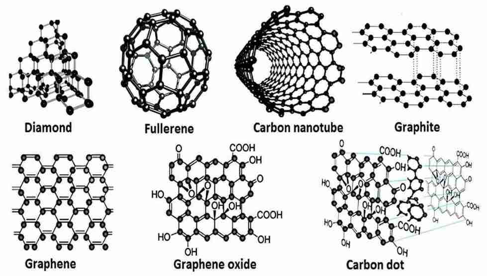
- Graphene is an allotrope (form) of carbon consisting of a single layer of carbon atoms arranged in a hexagonal lattice.
- It is nearly transparent.
- It is the basic structural element of many other allotropes of carbon, such as graphite, charcoal, carbon nanotubes, and fullerenes.
- Its thin composition and high conductivity mean it is used in applications ranging from miniaturized electronics to biomedical devices.
- The one-atom-thick sheets of carbon conduct electrons better than silicon and have been made into fast, low-power transistors. Researchers have measured the intrinsic strength of graphene, and they’ve confirmed it to be the strongest material ever tested.
Applications of graphene:
- Graphene is widely used in making solar cells, light-emitting diodes, touch panels, and smart windows. Graphene supercapacitors serve as energy storage devices with a capacity for faster charging and a longer life span than traditional electrolytic batteries.
- Other potential applications of graphene include water filtration and purification, renewable energy, sensors, personalized healthcare, and medicine, etc.

Carbon Nanotubes
Carbon nanotubes (CNTs) are an allotrope (Not isotope) of carbon.
- They take the form of cylindrical carbon molecules and have novel properties that make them potentially useful in a wide variety of applications in nanotechnology, electronics, optics, and other fields of materials science.
- They exhibit extraordinary strength and unique electrical properties and are efficient conductors of heat.
- Inorganic nanotubes have also been synthesized.
- Nanotubes are members of the fullerene structural family, which also includes buckyballs. Whereas buckyballs are spherical, a nanotube is cylindrical, with at least one end typically capped with a hemisphere of the buckyball structure.
- Their name is derived from their size, since the diameter of a nanotube is on the order of a few nanometers (approximately 50,000 times smaller than the width of a human hair), while they can be up to several millimeters in length.
- There are two main types of nanotubes: single-walled nanotubes (SWNTs) and multi-walled nanotubes (MWNTs).
Fullerenes
Buckminsterfullerene C60, also known as the buckyball, is a representative member of the carbon structures known as fullerenes. Members of the fullerene family are a major subject of research falling under the nanotechnology umbrella.
Fullerenes are also called Buckyballs due to their shape.
- Buckyballs may be used to trap free radicals generated during an allergic reaction and block the inflammation that results from an allergic reaction.
- The antioxidant properties of buckyballs may be able to fight the deterioration of motor function due to multiple sclerosis.
- Combining buckyballs, nanotubes, and polymers to produce inexpensive solar cells that can be formed by simply painting a surface.
- Buckyballs may be used to store hydrogen, possibly as a fuel tank for fuel cell-powered cars.
- Buckyballs may be able to reduce the growth of bacteria in pipes and membranes in water systems.
- Researchers are attempting to modify buckyballs to fit the section of the HIV molecule that binds to proteins, possibly inhibiting the spread of the virus.
- Making bulletproof vests with inorganic (tungsten disulfide) buckyballs.
You May Also like to Read: Triboelectric Nano Generator

